Theory
Transistor
The function of the transistor (from the English words TRANSfer resISTOR) is already indicated in its name – the transformation of resistance. Its discovery in 1947 caused a revolution in electronics and all related fields. Transistors are distinguished according to the type of charge carriers involved in the current conduction:
Bipolar, the essence of which is controlled by injection of minority carriers in the emitter base and subsequent extraction of carriers collector, where the current conducting participate both charge carriers – electrons and holes.
Unipolar, whose working principle is based on the interaction of the conductive channel between the emitter and the collector transverse electric field (Field Effect Transistor – FET), the current conduction in the channel is performed by one type of charge carriers (channel N – electrons, channel P – holes).
Bipolar Transistor
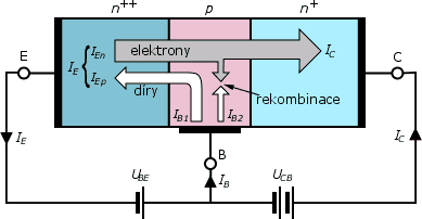
The bipolar transistor is an electronic component formed by the three areas of semiconductors with different types of conductivity arrangements NPN or PNP, which form a pair of PN junctions. The transistor has three electrodes and a base (used to control the transistor), the collector and the emitter. The base is compared to other much thinner electrodes (up to 100 times). The emitter is compared to the collector, which has the same conductivity type but is more heavily doped. The transistor is used as a signal amplifier or as a switch. It is also part of many other devices, such as logic circuits. The use of unipolar transistors predominates in complex integrated circuits.
The Transistor Effect
The ability to amplify the power transistor is called the transistor effect, which is an essential characteristic of the transistor. After applying a positive voltage to a negative collector and the emitter electrode of the transistor passes only a very small current in order nanoampér (This current increases with temperature). To bring more current through transistor must be based on through resistor positive voltage. This will open a transition base – emitter (There must be at least a voltage of 0.7 V). For NPN transistor base current flows into the holes. Since the base is very thin and fills quickly, holes from the emitter to the electrons start to flow. Some travel through the base to the positive pole of the source, but the majority are clamped to the positive voltage at the collector of the transistor and thus pass through the collector current, which is many times greater than the base current.
The higher the base current, the higher the collector current. This can be explained by the fact that the base current increases as the number of free charge carriers increases, and thus the resistance of the transistor decreases, resulting in an increase in the collector current as the voltage between the collector and emitter decreases. When the voltage drops to the level of a few tenths of a volt, the transistor is said to be saturated. In this state, it passes a relatively large current with negligible power dissipation. The saturation state is used when the transistor is working as a switch. If we apply a constant base current to increase the voltage between the collector and emitter, the collector current will initially increase rapidly and eventually stabilize at a nearly constant value, and the transistor begins to behave as a constant current source (see output characteristics).
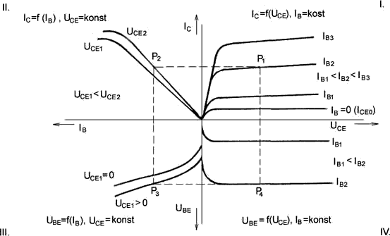
Graphical Representation of Characteristics
The output characteristics are plotted in the first quadrant of the curve. The magnitude of the output collector current increases with the growth of the base current.
The direction of the so-called transfer (current) characteristics in the second quadrant shows the current gain coefficient β.
The so-called input characteristics are shown in the third quadrant. The dependence of the input characteristics on the voltage UCE is minimal, therefore the input characteristics are often determined for a single value of UCE.
The dependence of the input voltage on the output is shown in the fourth quadrant in the form of the so-called reverse voltage transfer characteristic for different values of the base current.
Bipolar Transistor Characteristics
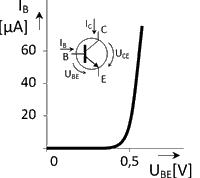
Input Characteristic
Input characteristics show dependence on the base current voltage between base and emitter. This is indicative of some voltage between the collector and emitter. Their shape corresponds to the current-voltage characteristics of diodes, as measured voltage and current in a PN junction.
From these characteristics, the h11 parameter can be determined, i.e. the input resistance.
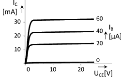
Output (Collector) Characteristic
The output characteristics of the dependence of the collector current on the voltage between the collector and emitter, while a constant base current. With increasing base current increases the maximum achievable collector current, as the base current resistance affects the entire transistor.
From these characteristics, parameter h22, the output conductivity, can be determined.
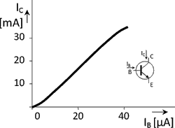
Transfer (Current) Characteristic
The transfer characteristic specifies the dependence of the collector current on the base current. It is reported to some voltage between the collector and emitter. Using this characteristic you can define a parameter h21 (also β), which is the current amplification coefficient.
Current Gain Coefficient
The current gain coefficient h21 (or β) is defined as the ratio of the change in the collector current to the change in the base current of the output short, i.e. at zero voltage change UCE.
Reverse Characteristics
These characteristics indicate the dependence of the voltage between the base and emitter voltage between the collector and emitter, while a given base current. Therefore, they describe the backhaul voltage from output to input. From these characteristics can be determined hybrid parameter h12, it is reverse voltage transfer.
The reverse characteristic is generally not measured, but constructed based on the input characteristic.